Microelectronic Design, Emulation, Fabrication & Validation
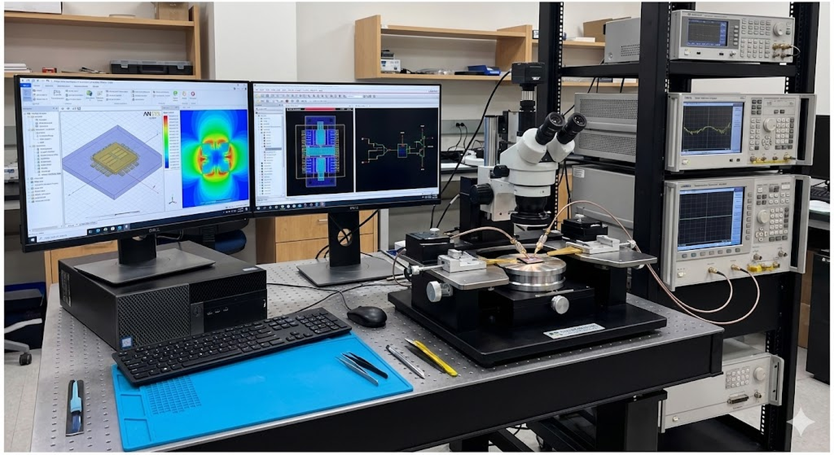
Executive Summary
This facility supports an end-to-end microelectronic workflow—from IC/RF front-end design and pre-silicon emulation, through fabrication handoff, to post-silicon validation and correlation.
Tool pillars
- EM & high-frequency verification: ANSYS Electronics Desktop / HFSS
- Custom IC schematic-to-layout: Cadence Virtuoso (PDK-based)
- System/channel realism for wireless experiments: Remcom Wireless InSite
New project? Start with Quick Start, then follow the Recommended end-to-end workflow.
Navigation
- Capabilities
- Quick Start
- Tool map
- HFSS
- Virtuoso
- Wireless InSite
- Recommended end-to-end workflow
- Checklists & best practices
- Notes for students and new lab members
Capabilities
Design
- Analog / mixed-signal / RF IC schematic design and simulation
- RF/microwave modeling (antennas, passives, packages, interconnects)
- Co-design of circuits + EM structures + system constraints
Emulation
- Pre-silicon exploration using behavioral/compact models
- Parameter sweeps and sensitivity studies to de-risk tapeout
- “What-if” studies on corners, parasitics, and layout-dependent effects
Fabrication handoff
- Layout readiness checks (DRC/LVS/PEX workflows via PDK)
- Tapeout package preparation (GDS + documentation)
- Coordination for MPW/shuttle or foundry pathways (availability depends on project and partner access)
Validation
- Post-silicon comparison: measured vs simulated
- S-parameter correlation, de-embedding planning, and model updates
- Reproducible reporting for publications and future tapeouts
Quick Start
Pick your entry point
- EM/RF components & antennas → HFSS
- IC schematic-to-layout → Virtuoso
- Propagation / RIS / channel realism → Wireless InSite
Build a minimal, reviewable baseline (aim for 1–2 days)
- One schematic or EM model that reproduces a known reference
- One plot that becomes your golden regression (S-parameters, gain, NF, phase noise, etc.)
Decide your validation target early
- What will be measured? what fixtures? what calibration/de-embedding approach?
Tool map
| Tool | Best for | Typical outputs |
|---|---|---|
| ANSYS AEDT / HFSS | 3D EM simulation of antennas, passives, packages, interconnects | S-parameters, radiation patterns, fields, loss/Q, EM co-sim models |
| Cadence Virtuoso | IC design from schematic → layout → verification → sign-off | Schematics, simulations, layout, DRC/LVS/PEX reports, GDS |
| Remcom Wireless InSite | Site-specific channel realism via ray-tracing / empirical models | Coverage maps, channel impulse response, path loss, multipath statistics |
ANSYS Electronics Desktop & HFSS

Best for: EM simulation and validation of RF/microwave components, antennas, and high-frequency structures using 3D FEM workflows.
Self-paced resources
- ANSYS Academic Learning Resources: https://www.ansys.com/academic/learning-resources
- Intro course (HFSS workflows & fundamentals): https://innovationspace.ansys.com/product/intro-to-ansys-hfss/
- Antenna learning track: https://innovationspace.ansys.com/courses/learning-track/fundamentals-of-antenna/
- Student Version (non-commercial): https://www.ansys.com/academic/students/ansys-electronics-desktop-student
- Learning Library & Forum: https://innovationspace.ansys.com/learning-library/
Structured / premium resources
- ANSYS Learning Hub: https://www.ansys.com/services/ansys-learning-hub
- SimuTech EMAG102 (3D EM design): https://simutechgroup.com/services/ansys-training/emag-102/
- Rescale batch/HPC tutorial: https://rescale.com/documentation/main/ansys-resources/ansys-hfss/ansys-hfss-batch-tutorial/
Research-oriented learning path
- Install AEDT (student version where appropriate).
- Complete the Intro HFSS course.
- Reproduce at least one reference antenna/passive example.
- Modify: substrate, port type, mesh/convergence settings.
- Capture convergence evidence and solver settings.
- Add parametric sweeps and HPC workflows as needed.
Practical tips
- Ports/boundaries + mesh/convergence dominate result quality—treat them as first-class design artifacts.
- Save convergence plots and solver settings for paper-quality reproducibility.
- Consider related AEDT tools (Q3D, SIwave, Icepak) when SI/PI/thermal coupling matters.
Cadence Virtuoso

Best for: custom IC design (analog, mixed-signal, RF) from schematic capture to layout, verification, and simulation.
Official training
- Virtuoso Schematic Editor S1 (schematics): https://www.cadence.com/en_US/home/training/all-courses/84443.html
- Virtuoso Layout Design Basics: https://www.cadence.com/en_US/home/training/all-courses/84460.html
- Online Training Library: https://www.cadence.com/en_US/home/training/deliverymethod-online.html
- SKILL programming: https://www.cadence.com/en_US/home/training/all-courses/83018.html
University and open tutorials
- University at Buffalo tutorial: https://www.acsu.buffalo.edu/~ajr33/cse-493_593/VirtuosoTutorial.html
- Virginia Tech tutorial: https://www.mics.ece.vt.edu/ICDesign/Tutorials/Cadence/index_old.html
- UBC inverter design (45 nm): https://sudip.ece.ubc.ca/cadence-virtuoso-schematic-simulations/
- Community playlist (YouTube): https://www.youtube.com/playlist?list=PLjRIBQDeKyRrPh4TXxroprf2h4bjkYdRW
Academic/community access
- CMC Microsystems (academic suite access): https://www.cmc.ca/cadence-for-teaching/
From zero to tapeout-ready
- Reproduce a “hello world” design (e.g., inverter/op-amp) in a standard PDK.
- Learn simulation flows: DC/AC/transient, corners, and basic Monte Carlo.
- Transition to layout and run DRC/LVS.
- Add PEX, then compare pre/post-layout results.
- Automate repetitive tasks with SKILL only after the manual flow is stable.
Practical tips
- Define sign-off checks early (DRC/LVS/PEX/corners/Monte Carlo) and keep them consistent.
- Maintain a versioned tapeout checklist (schematic, layout, verification reports, notes).
Remcom Wireless InSite

Best for: RF propagation modeling via 3D ray-tracing and empirical models to predict coverage, channel characteristics, and system performance in realistic environments. We often use it for testbed planning and RIS-assisted communications studies.
Official tutorials and videos
- Indoor Propagation Analysis tutorial: https://www.remcom.com/resources/video/wireless-insite-indoor-propagation-analysis-tutorial
- Intro series (floor plans / geometry): https://www.remcom.com/resources/video/wireless-insite-intro-series-creating-and-editing-indoor-floor-plans
- Dynamic mobility simulation: https://www.remcom.com/resources/video/simulate-dynamic-wireless-mobility-with-wireless-insite
- Product overview & features: https://www.remcom.com/wireless-insite-propagation-software
Documentation and support
- Remcom simulation support & training: https://www.remcom.com/electromagnetic-simulation-support
- Reference PDF (User’s Guide 2.7.1): https://www.stud.usv.ro/NACRC/NACRC/P1/Wireless_InSite_Users_Guide.pdf
Channel realism learning path
- Run the indoor tutorial to understand the ray-tracing workflow.
- Build/import a simple environment and assign materials.
- Generate coverage maps and channel outputs; sanity-check with simplified baselines.
- Add mobility/time variation if your experiment needs it.
- Export results for MATLAB/Python post-processing (plots, statistics, comparisons).
Practical tips
- Treat geometry + material definitions as the model—document them like a circuit schematic.
- Record frequency bands, antenna patterns, and material properties for reproducibility.
Recommended end-to-end workflow
- Concept + requirements
- Target frequency, bandwidth, power, sensitivity, interfaces, and measurement plan
- Pre-silicon modeling / emulation
- Behavioral models → schematic simulations → early EM checks
- Layout + verification
- DRC/LVS/PEX + correlation against schematic intent
- EM co-simulation (as needed)
- Packages/interconnects/antennas/passives + parasitics
- Fabrication handoff (project-dependent)
- GDS + documentation + sign-off checklist + versioned deliverables
- Post-silicon validation
- Calibration/de-embedding + measured vs simulated correlation
- Documentation
- Store tool versions, scripts, and “golden” plots to ensure publishable, repeatable results
Checklists & best practices
Tapeout-readiness (typical)
- ✅ DRC clean + reports archived
- ✅ LVS clean + connectivity assumptions documented
- ✅ PEX completed + pre/post-layout deltas reviewed
- ✅ Corner coverage defined (PVT, mismatch/Monte Carlo as appropriate)
- ✅ Foundry deliverables packaged (GDS + runsets + README + version tags)
Measurement-correlation (typical)
- ✅ Fixture and calibration plan (SOLT/TRL/etc.) selected before the first measurement run
- ✅ De-embedding approach defined (structures, reference planes, uncertainty notes)
- ✅ Measured vs simulated plots use the same reference planes and same conditions
- ✅ Model updates are traced to measurements (revision history + rationale)
Reproducibility basics
- Keep a lab notebook + version control for projects, scripts, and plots.
- Save tool versions, PDK versions, and solver settings with every “golden” plot.
Notes for students and new lab members
- Start small: one reproducible result beats ten half-working models.
- Ask for help with: tool version, screenshots, the smallest reproducing case, and expected vs observed behavior.
- Treat setup details (ports, boundaries, runsets, fixtures) as part of the design—not an afterthought.
Access & support
Who this is for
- Students and researchers doing IC/RF design, EM validation, and post-silicon correlation
- Projects that need a documented path from simulation assumptions → fabrication deliverables → measured results
When requesting help, include
- Tool + version (and PDK version if using Virtuoso)
- The smallest reproducing case (project archive or screenshot series)
- What you expected vs what you observed
- Any “golden” plot you are trying to match (and how it was generated)
Recommended project folder skeleton
00_requirements/(spec, interfaces, measurement plan)10_models/(behavioral/compact models)20_schematic/(schematic + sims)30_layout/(layout + DRC/LVS/PEX reports)40_em/(HFSS projects, ports/boundaries notes, convergence evidence)50_fab/(GDS, runsets, README, sign-off checklist)60_measurement/(fixtures, calibration notes, raw data)70_correlation/(measured vs simulated plots, model updates)
Collaboration norms
- Assume every result should be reproducible by someone else in 6 months.
- Treat runsets, ports/boundaries, and calibration steps as design artifacts.
- If a project is headed toward tapeout, plan a review gate for: spec freeze → pre-layout sign-off → post-layout sign-off → handoff package.